
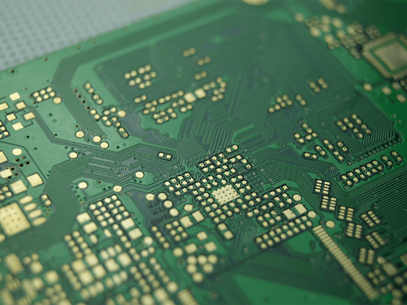
Full Range of PCB Capabilities to Fit Your PCB Manufacturing Needs
UETPCBA specializes in the prototype and production of high-end double-sided/ multi-layer circuit PCB circuit boards. PCB products include 1-48 layers board, HDI PCB, high TG thick copper PCB, high frequency PCB, Rogers mixed-lamination PCB, blind/buried vias PCB, metal base PCB, half hole PCB, gold-finger PCB, impedance control PCB, countersunk hole PCB, high frequency antenna PCB, etc. Our core competitiveness is leading PCB technology, high-end PCB capabilities production technology, high-quality PCB products, on-time delivery, consultant customer service and optimal cost.
In the field of high-end printed circuit board manufacturing, we always maintain efficient delivery capabilities, combined with the high quality of production management, research and development PCB manufacturing capabilities, manufacturing capabilities and construction of PCB core technologies, accelerating technological innovation and development.
Listed below are UETPCBA’s PCB manufacturing capabilities. We are focused on providing high-quality printed circuit boards to fit all of your needs.
Detailed Printed Circuit Board Assembly Capabilities
| Standard Features | Standard | Advanced |
|---|---|---|
| Maximum Layer Count | 20 | 48 |
| Maximum Panel Size | 533x610mm [21×24″] | 610x1067mm [24×42″] |
| Outer Layer Trace/Spacing | 90µm/90µm | 64µm/76µm |
| (1/3oz starting foil + platig) | [0.0035″/0.0035″] | [0.0025″/0.003″] |
| Inner Layer Trace/Spacing | 76µm/76µm | 50µm/50µm |
| (Hoz inner layer cu) | [0.003″/0.003″] | [0.002″/0.002″] |
| Maximum PCB Thickness | 3.2mm [0.125″] | 6.5mm [0.256″] |
| Minimum PCB Thickness | .20mm [0.008″] | .10mm [0.004″] |
| Minimum Mechancial Drill Size | .20mm [0.008″] | .10mm [0.004″] |
| Minimum Laser Drill Size | .10mm [0.004″] | .08mm [0.003″] |
| Maximum PCB Aspect Ratio | 10:1 | 25:1 |
| Maximum Copper Weight | 5 oz [178µm] | 6 oz [214µm] |
| Minimum Copper Weight | 1/3 oz [12µm] | 1/4 oz [9µm] |
| Minimum Core Thickness | 50µm [0.002″] | 38µm [0.0015″] |
| Minimum Dielectric Thickness | 64µm [0.0025″] | 38µm [0.0015″] |
| Minimum Pad Size Over Drill | 0.46mm [0.018″] | 0.4mm [0.016″] |
| Solder Mask Registration | ± 50µm [0.002″] | ± 38µm [0.0015″] |
| Minimum Solder Mask Dam | 76µm [0.003″] | 64µm [0.0025″] |
| Copper Feature to Edge, V‐cut (30°) | 0.40mm [0.016″] | 0.36mm [0.014″] |
| Copper Feature to PCB Edge, Routed | 0.25mm [0.010″] | 0.20mm [0.008″] |
| Tolerance on Overall | ± 100µm [0.004″] | ±50µm [0.002″] |
| Dimensions |
| HDI Features | Standard | Advanced |
|---|---|---|
| Minimum Microvia Hole Size | 100µm [0.004″] | 75µm [0.003″] |
| Capture Pad Size | 0.25mm [0.010″] | 0.20mm [0.008″] |
| Glass Reinforced Dielectrics | Y | Y |
| Maximum Aspect Ratio | 0.7:1 | 1:1 |
| Stacked Microvias | Y | Y |
| Copper Filled Microvias | Y | Y |
| Buried Filled Vias | Y | Y |
| Maximum No. of Buildup Layers | 3+N+3 | 5+N+5 |