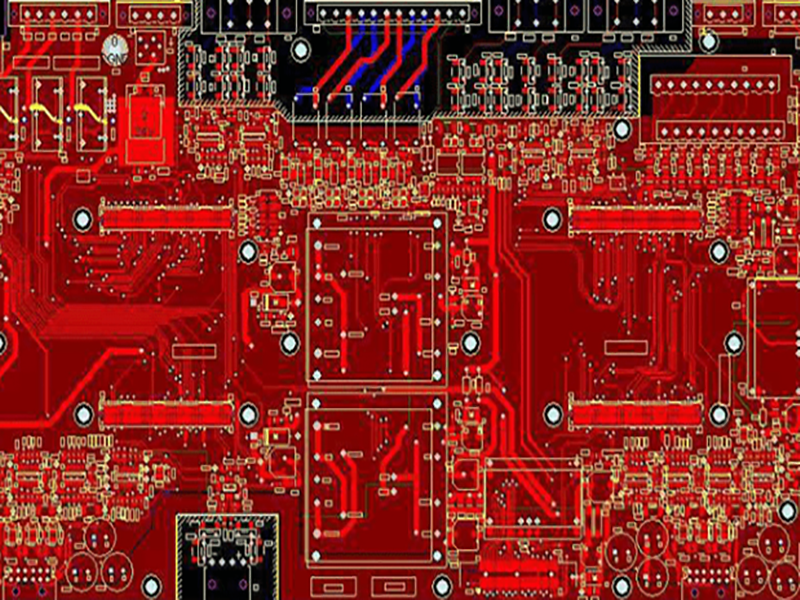
According to customers’ requirements from product concept, design to production, we are committed to providing customers around the world with one-stop product development solutions, winning the trust of customers with very competitive prices and quality services.

Our comprehensive PCB design services capabilities ensure a completed understanding of your project’s technical requirements and DFM ((Design for Manufacturability). Our PCB designs conform to the IPC 2200 standard and PCB assembly to IPC-A-610 standards.


Start A Quote Now

PCB Design ServicesCapabilities

  • Maximum PCB design layers:48layers
  • Maximum PIN count:110000+
  • Maximum connections:78000+
  • Minimum line width:2.4mil
  • Minimum line spacing:2.4mil
  • Minimum via size:4mil
  • Maximum BGA:60+
  • Minimum BGA PIN spacing:0.3mm
  • Maximum BGA PIN count:2912
  • Highest speed signal:56G-PAM4

Our PCB Design Services Advantages

Free to provide customers with PCB packaging construction, impedance calculation, PCB stack-up design, pcb board design, reverse engineering and EMC inspection.

Set up a discussion group for the project to ensure real-time communication and timely feedback on project progress, help customers shorten development cycle.

Complex design experience of high frequency, high density, high-speed, digital and analog mixing, multilayers, and HDI, impedance control, blind & buried vias, etc.

Experienced design team, from pcb board design to manufacturing process to provide turnkey solutions. Master the advanced technical information, full consideration of EMI/EMC and manufacturability design.

Provide optimization solutions of fully evaluate the design and manufacturability, and cost optimization of PCB manufacturing for customers.

High quality management system, standardized pcb board design management system and strict inspection, to ensure 100% satisfaction, 500+ customer reputation accumulation.

Compatible with popular design software including Altium Designer, Cadence, Allegro, Eagle and Pads.

High standard confidentiality measures, signing NDA agreement, exported files need to be approved, to ensure that the documents and project info are 100% confidential.

The Design Cycle

PIN count (single PCB)Design Cycle (Working Day)
≤10003-5
2000-30005-7
4000-50008-12
6000-700012-15
8000-900015-18
10000-1300018-20
14000-1500020-22
16000-2000022-30

PCB Design Workflow

01

Providing Information

Schematic: Generates the correct Netlist (eg: schdoc, sch or DSN)Structure diagram (DXF): Provide the specific position and direction identification of the components.BOM: Determine and check the specific package information on the schematic.Design guide: Description of specific signal, design requirements for impedance, stack-up, etc.

02

Layout Evaluation by UETPCBA

According to the design specifications, design instructions, design requirements and relevant checklists, our engineers will proceed with the schematic DRC inspection, structural verification and other electrical design requirements. Will feedback to customers if there is any problem..

03

Layout Confirmation by Customer

After finishing the preliminary layout, we will provide layout and structure files for customer review, so that customers can confirm the layout rationality. (eg: stack-up, impedance, structure, package, component placement and routing parameters.

04

Layout Data Output

After completing PCB Layout and getting confirmation from customers, our engineers will perform DFM inspection, QA inspection and EMC inspection. Then will export the production documents to customers including PCB source files, Gerber files, assembly files, structure files, etc.