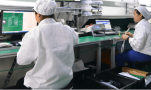
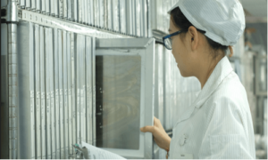
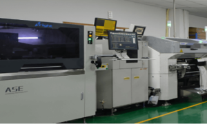
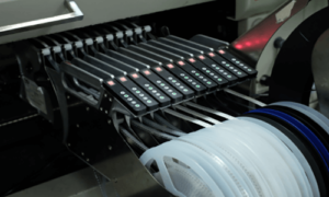
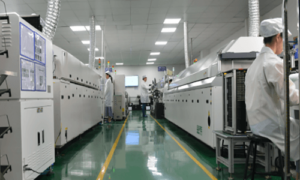
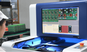
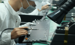
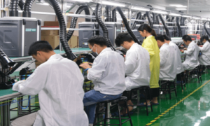
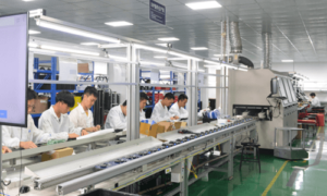
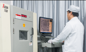
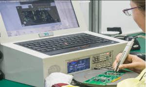
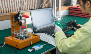
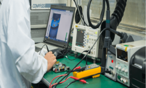
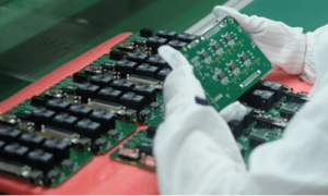
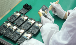
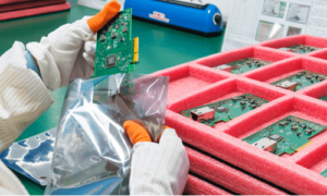
PCBA Process

We have 8 fully automatic SMT production lines, 4 DIP/ Through-Hole insertion lines and 2 wave soldering lines, as well as other advanced production equipment. UETPCBA strictly controls PCBA process flow under the guidance of ISO9001 quality system and IPC-A-610E standard to ensure the stability of the production process and reliable product quality.

Start A Quote Now

1

IQC Incoming Material Inspection

The first step of printed circuit board assembly process flow is importtant. The purpose of incoming material inspection is to prevent poor quality and delay delivery from defective materials. We should make sure the PCB boards are correct and the incoming components are consistent with BOM to be soldered.

2

Solder Paste Printing

It’s a key part of the surface mount pcba process flow, applying solder paste to a printed circuit board (PCB), the most common option of applying solder paste to a PCB through a stencil printer. This process deposits accurately the correct amount and thickness of solder onto solder pads.

3

Solder Paste Inspection (SPI)

Solder paste inspection aims to find out the defective solder paste printing online in the Printed Circuit Board (PCB) assembly process. SPI can directly check the quality of solder paste on PCBs, and provide a hint of the types of defects. With the help of solder paste inspection, manufacturers can reduce the defects rate and save significant costs and time.

Start A Quote Now

4

SMD Component Placement

Component placement is an electronics manufacturing pcba process flow that install surface assembly components accurately to the fixed position on printed circuit boards (PCBs) to create electrical interconnections between components and PCBs. The equipment used is SMT Pick& Placement machine.

5

Reflow Soldering

The process of reflow soldering is using solder paste to temporarily attach electrical components through their contact pads, after a prolonged period of high temperatures to melt the solder paste and make the surface assembly components firmly adhere to the PCB board. The solder paste reflows in a molten state, creating permanent solder joints.

6

Automated Optical Inspection (AOI)

Automated optical inspection (AOI) is an automated visual inspection of printed circuit board based on optical principle to detect common defects in PCB assembly production. Where a camera will automatically scan the PCB, collect images, check the defects (e.g. missing parts, wrong parts, etc.) on the pcb design flow after compared with parameters set in the database, and mark the defects through the display for maintenance personnel to repair.

Start A Quote Now

7

Repair

The PCBs that do not pass AOI inspection will be sent to maintenance personnel for repair until they rework according to the effects which last step marked. The tools used are soldering irons, repair workstations, etc.

8

Through-Hole Component Soldering

Some PCBs require through-hole components as well in conjunction with the common SMD components, through-hole technology used for electronic components that involves the use of leads on the components that are inserted into holes drilled in printed circuit boards and soldered to pads on the opposite side either by manual soldering, wave Soldering or the automated insertion mount machines.

9

Wave Soldering

Wave soldering is used in through-hole printed circuit assemblies and surface mount process of printed circuit boards for bulk production. The PCBs are passed over a pan of molten solder to make the soldering surface of the through holes directly contact with molten solder. As the circuit board makes contact with this wave, the components achieve soldered to the board.

Start A Quote Now

10

X-Ray Inspection

X-Ray Inspection is commonly performed on Quad-flat No-lead (QFN) and Ball Grid Arrays (BGAs) components in Printed Circuit Board Assembly process to find hidden assembly defects.

11

First Article Inspection

First article inspection is one of the most important processes in PCBA manufacturing to guarantee the quality of assembly. In this process, the BOM, coordinate, designator or sample picture will be loaded into the application to generate a test program. The LCR measuring instrument will automatically compare the value of components and generate the inspection report.

12

IC Programming

IC programming is the process of transferring a computer program into an integrated circuit. After PCBA production, there are several different ways to do IC programming. UETPCBA provides offline programming and online programming.

Start A Quote Now

13

Functional Test

Printed circuit board functional testing is performed at the end of the PCBA manufacturing process to test the functionality of the PCB, and ensure whether the electrical characteristics and performance work well as expectations.

14

Visual Inspection

The assembled board must be visually inspected according to IPC – 610 inspection standard. Standardize finished product inspection to ensure soldering quality and no defective boards to be shipped.

15

PCBA Cleaning

For the final production of Printed Circuit Boards, the process of cleaning is needed to remove soldering residue such as flux, dust and solder beads on the assembled PCB. After finishing the cleaning, then we can go to the next step of packing.

Start A Quote Now

16

PCBA Packing

Before shipping, special PCBA packaging is required to prevent damage during transportation and ensure that the final PCBA board delivered to the customer is in good condition. All our pcba manufacturing process products are shipped with anti-static ESD packaging to prevent chips being broken by static electricity as well as customized carton to fix the boards and prevent shaking.