Quality Management
Under the guidance of ISO9001 quality system, IPC-A-610E standard and SPC control method to improve quality system and fabrication equipment. We strictly control PCB design process, DFM checking, new product introduction, PCBA manufacturing, supply chain management, PCBA testing and personnel training to form a quality management system to ensure the stability of the production process and quality assurance.

Pre-production Check:
Confirm final file version
Confirm PCB specifications: material, thickness, copper thickness, layers, stack-up, finish surface, solder mask and so on.
Correct designators of components and clear silkscreen with orientation
Complete component descriptions of manufacturer, P/N, designator and QTY in BOM
Correct pick & place file
SMT Process: with lead/lead-free
Complete procedure of programming and function test
Other special requirements
New Product Introduction:
Hold a new product introduction meeting with sales, engineering, production, purchasing and quality department.
Make clear customer’s requirements, product application, lead time and other special technical requirements
Record into production system and generate Internal & customer PN
Evaluation of manufacturing difficulty and key quality control points of the project
Clear Lead time of PCB fabrication, PCB assembly and components procurement
Make production & test plan
PCB Manufacturing:
High quality raw material guarantee
High-end manufacturing capabilities
Advanced production & test equipment
Professional technical team
All PCB 100% electrical test
Components Procurement:
100% original parts as specified follow customer’s BOM
Purchase from original manufacturer, authorized distributor and other formal channels
Provide perfect original technical support & COC
Shorter procurement cycle, stock advantages
Provide cost down solutions in long term
Incoming Material Quality Control:
PCB checking: measurement of PCB Thickness, through hole if non-plated or covered with solder mask, Pads if flat and clean, silkscreen if clear, if PCB warped, scraped and broken
Check the PN, QTY and silkscreen of incoming components if they are consistent with BOM
The incoming components are placed on the bare board for the fit test
Check the value of resistors and capacitors and compare them with BOM
Check whether there are scratches, deformations, broken pins, short pins on the surface of incoming components.
Component Storage & Solder Paste Printing:
Professional constant temperature and humidity cabinet to save sensitive components
Bake the PCB/IC/BGA for 2-12 hours to remove the moisture on the surface and enhance the solderability
Select high-quality manufacturers of solder paste, such as Alpha-fry
Free provide high quality laser SMD stencil
Equipped automatic solder paste printer and SPI to ensure consistency and reliability
SMT Assembly:
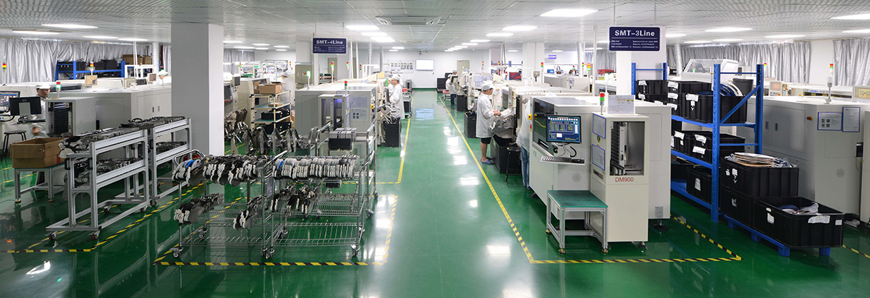
Yamaha and FUJI high speed automatic SMT pick* place machine, up to 01005
Major chip types such as QFN, SOP, SOT, TSOP, QFP, BGA, PLCC are available
Automatic optical inspection (AOI) to detect wrong & missing parts, reverse
& false soldering and other defects
X -Ray inspection to check soldering effects of balls
All PCBA boards will be 100% test
Warranty:
(I)PCB bare boards: UETPCBA provide warrants for bare PCB boards against defects in materials and workmanship under normal use for a period of 90 days from date of shipment. If a defect arises and a valid claim is received within the warranty period, return the bare boards. UETPCBA provide two solutions: re-fabricate the bare board at no charge or issue a credit equal to the original order price.
UETPCBA will not accept liability for any cost in addition to the value of the bare boards including but not limited to components, labor, business interruptions and any other consequential damages or losses.
(II)PCBA boards: We will include the cost of any components UETPCBA supplied and all labor that we supplied with regard to replacing the assemblies or issuing a credit.
This limited warranty does not apply:
(A) Damage caused by use with non-UETPCBA products and services;
(B) Damage caused by accident, abuse, misuse, flood, fire, earthquake or other external causes;
(C) Product or component that has been modified to alter functionality or capability without the written permission of UETPCBA;
(D) Appearance damage, including but not limited to scratches or dents, does not affect the product’s functionality or materially impair its use.

