What is High Frequency PCB?
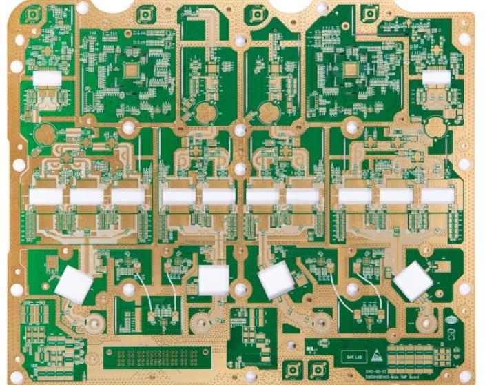
A high frequency printed circuit board is a special PCB with high electromagnetic frequency, high frequency can be defined as the frequency above 1GHz. High frequency pcb has high requirements for physical performance, accuracy and technical parameters. It is widely used in automobile collision avoidance systems, satellite communications, wireless networks and other fields. The basic characteristics of high frequency PCB materials are required as follows:
- The thermal expansion coefficient of high frequency PCB materials and copper foil should be consistent, otherwise, it is easy to cause the separation of copper foil.
- High frequency pcb requires a small dielectric constant (DF) to ensure signal transmission quality.
- The dielectric constant (DF) is required to be small to ensure the quality of signal transmission.
- The water absorption of high frequency PCB material should be as low as possible.
- High frequency PCB material requires good heat resistance, electrical properties, chemical stability, peel strength, etc.
- With the increase of power signal frequency, the loss on the PCB substrate is very small.
Advantages of High Frequency PCB Manufacturing
High Speed: The high frequency PCB material with a small dielectric constant, and the corresponding signal transmission speed will be faster,
High Efficiency: generally speaking, the high frequency printed circuit board with a small dielectric constant, the loss will be very small, which can high-efficient achieve the needs of the target heating.
Better Regulation: high frequency printed circuit board can achieve different depths of components heating, and can easily complete local or centralized heating.
Strong Resistance: because the water absorption of high frequency PCB materials is very low, so this kind of circuit board has good chemical corrosion resistance, moisture resistance, high-temperature resistance, as well as great peel strength, and many other advantages.
PCB Design Skills for High Frequency PCB
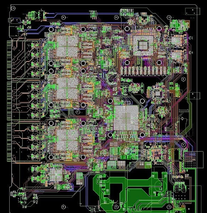
With the wide application of printed circuit boards, as well as the development and innovation of electronic technology, high frequency, high speed, and high-density PCB manufacturing of modern electronic products has been developed rapidly. The PCB industry is going to micro-hole and buried/blind hole, uniform thin dielectric layer. The PCB design technology of high frequency, high speed, and high-density multilayer PCB has become an important research field. Now the PCB design mainly tend to small size, easy fabricate to save cost. Each interconnection point should be investigated and the existing problems should be solved in RF PCB design. The interconnection of the circuit board system includes chip to the circuit board, interconnection within PCB board, and signal input/output between PCB and external device.
The skills of high frequency PCB design are shared in the following:
- The high-performance insulated circuit board should be strictly controlled according to the level of insulation constant value.
- The design specification of high frequency PCB with high precision etching should be improved.
- Avoid components with leads, at high frequency pcb, it is best to use the surface-mounted assembly components.
- To avoid the use of through holes (PTH) on the sensing board, the fewer through holes (VIA) used during component connection, the better.
- Maintain signal transmission integrity, as well as good signal impedance matching
- To provide a rich layer to prevent the impact of a 3D electromagnetic field on the high frequency pcb.
- The ground lines of high frequency digital signal and analog signal need to be isolated to reduce noise interference.
- The wiring of the differential pair should pay attention to the two lines should be the same length, and the distance between the two lines should be kept parallel.
- When applying copper to the high-speed signal line, we should pay attention to the distance between the copper and the signal line, and not affect its characteristic impedance.
- High frequency circuit with high wiring density, try to use multilayer wiring, also can effectively reduce the interference.
- DDR, LVDS, USB, HDMI, and other high frequency signal line design as short as possible, because the longer the high frequency signal lead, it is easier to coupling to its components up.
- High frequency signal wiring as far as possible not to form a loop.
- High frequency circuit wiring leads the best full straight line, the transmission line corner to use 45° Angle, to reduce the high frequency signal external transmission and coupling between each other.
- Adding a high-frequency uncoupling capacitor to the power pin of the IC block can effectively suppress the interference caused by the high-frequency harmonics on the power pin.
Conclusion
With the rapid development of science and technology, more and more equipment is designed for applications in the microwave frequency band (>1GHZ) or even in the millimeter wave field (30GHZ). This also means that the frequency is getting higher and higher, and the circuit board is The requirements for materials are getting higher and higher. For example, the substrate material needs to have excellent electrical properties, good chemical stability, and the loss on the substrate with the increase of the power signal frequency is very small. With the emergence of 5G signals, the importance of high frequency pcb has emerged. The high frequency pcb manufacturing industry is also particularly important.