Overview
Electronic products have become an indispensable part of our daily life. The core of these electronic devices is the printed circuit board (PCB). If you are interested, take the electronic product apart and you can see the PCB. The printed circuit board with components installed is called an assembled circuit board, and its manufacturing process is called a PCB board assembly.
PCBA process can be said to be a simple and complex. Simple because
pcba process consists of only a few manual and automatic steps, the whole pcba process is very simple. The complexity is because every PCBA process step is critical, and even a little offset may cause catastrophic results. To help you better understand the PCB assembly process, we will explain each step of the operation process in detail in this article for your reference.
PCB assembly technology
There are two main types of modern PCB assembly technology: surface mount technology (SMT) and through hole technology (THT). PCB assembly technology is different, and PCB process is also different.
- SMT
Mainly used in sensitive components, very small resistance. Through SMT, these components are automatically placed on the surface of the circuit board and are called surface mount devices.
- THT
Suitable for components with wires or pins, these components must be installed on the circuit board by inserting them into the holes on the circuit board. Through-hole technology is applied to pcb board assemblies containing large components.
Preparation work before pcb board assembly
Before the pcba process officially starts, it is necessary to make some preparations. This helps the circuit board manufacturer to evaluate the function of the circuit board design, which is mainly reflected in the design for manufacturability (DFM) inspection.
- Price
- Purchasing and Bill of Materials (BOM)
- ESD precautions
- Electronic component kit
- Dry cabinet storage
- CAD/CAM programming
PCBA process about SMT
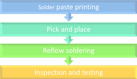
- pcba process about SMT picture format
-
Solder paste printing
The first step of SMT assembly is to apply solder paste evenly on the circuit board, specifically, on the pads of the components. The precise coating benefits from the stainless steel mesh, which is provided with precise leaks according to the circuit board design documents. When the solder paste is printed, the solder paste will be accurately coated on the material pad. The pressure, angle and speed of the squeegee will test the technology and experience of the circuit board assembly manufacturer. Once any link is improperly handled, solder paste printing cannot be considered successful.
In the professional PCBA process flow, first, the mechanical fixture fixes the circuit board and the steel mesh in place, and then the applicator places the solder paste precisely on the predetermined area. Next, the machine spreads the solder paste on the stencil and evenly spreads it on each open area. Finally, after removing the stencil, the solder paste will remain in the predetermined position.
-
Pick and place
The second step of the pcba process is pick and place. After the solder paste is printed, the conveyor belt moves the circuit board to the pick and place machine, which places the surface mount components on the printed solder paste circuit board.
The pick-and-place machine picks up and places the material by picking up the circuit board with the vacuum fixture and moving it to the pick-and-place station. Then, the machine positions the circuit board on the stage, and then the component is placed on top of the solder paste in the pre-programmed position.
-
Reflow soldering
The third step of the pcba process is reflow soldering. Once the solder paste and surface mount components are all in place, it’s time to fix them on the circuit board. Circuit board assembly achieves this through a process called reflow. The solder paste is first melted at a high temperature, and then cooled and permanently solidified. In this way, surface mount components will be fixed on the surface of the circuit board.
Many circuit boards require special consideration during reflow, especially double-sided circuit board assembly. Double-sided printed circuit board assemblies require separate printing and reflow on each side.
-
Inspection and testing
Inspection and testing is a link that cannot be ignored in the pcba process. Once the surface mount components are soldered in place after reflow, this does not mean that the circuit board assembly is complete. The assembled circuit board needs to be tested for functionality. Usually, the movement during the reflow process can cause poor solder joints, or complete lack of connections, or even short circuits.
Common methods used to check for these errors and misalignments include:
- Manual inspection
- Automatic optical inspection
- X-ray inspection
These inspections can be carried out regularly after the reflow pcba process to determine any potential problems and risks. These regular checks can ensure that errors are discovered and fixed as quickly as possible. This helps manufacturers and designers save time, manpower, and material costs.
Functional testing is the last and most important step in the PCBA process because it determines the success or failure of all the previous assembly steps, and it is also the reason why regular testing and inspection in the entire PCBA process are so important.
PCBA process about THT
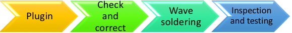
- pcba process about THT picture format
The printed circuit board THT assembly is the traditional assembly method of the circuit board, which becomes the through-hole technology assembly. Unlike SMT assembly which all relies on automatic procedures, the through-hole assembly process includes both manual procedures and automatic procedures.
-
Plugin
The first step of the pcba process is done manually by professional engineering personnel. The engineer needs to quickly and accurately place the electronic components in the corresponding position according to the customer’s pcb design file. The plug-in must comply with the regulations and operating standards of the pupil installation process to ensure the high quality of the end product.
-
Check and correct
The second step of the pcba process is check and correct. Once the plug-in is completed, the circuit board is placed in a transport frame in an area, and the circuit board into which the material is inserted will be automatically checked to determine whether the material is placed accurately. If problems with component placement are observed, it is easy to correct them immediately. After all, this is done before welding.
-
Wave soldering
The third step of the pcba process is wave soldering. After the material is correctly inserted into the circuit board, the through-hole components will be soldered to the circuit board. In the THT assembly process, wave soldering is used to complete the soldering process. In a wave soldering system, the circuit board slowly passes through a wave of liquid solder at high temperatures. After that, all wires or wire connections can be successfully obtained.
At the end of the PCBA process are the same as the SMT assembly process. The THT assembled and soldered circuit boards also need to be inspected and tested to ensure their accuracy and high quality.
After printed circuit board assembly
When you see a brand new printed circuit board, you will sigh its texture. But in fact, the pcba process is seemingly dirty. A certain amount of flux will be left in the solder paste printing process, and at the same time, the workers on the production line will also transfer fingerprints and dirt from clothes to the surface of the pcb.
If the flux is not cleaned up in time, the flux residue will become viscous after it is left on the PCB surface for several months, which will damage the solder joints over time. In addition, the dirt on the surface of the pcb will also affect the customer’s first impression of the product. Therefore, the printed circuit board should be cleaned up in time after soldering.
Summary
The above is a simple pcba process. In short, the quality of solder joints of electronic components determines the quality of pcb board assembly. With the continuous development of society and the continuous update of the technology, the failure rate is constantly decreasing, the pcba process will also be simplified. UETPCBA has rich experience in this area, if you have any questions, please feel free to consult us.