Instruction
Most PCBs in the past were relatively simple and were limited by manufacturing technology. While PCBs used for simple electronic devices with limited functionality were usually composed of single layers, more complex electronic devices (such as computer motherboards) were usually composed of multi-layer PCBs. But do you know how are multilayer pcbs manufactured and what is the multilayer pcb advantages? With the increasing complexity of modern electronic devices, these multilayer PCB boards are more common than ever before, and manufacturing techniques have reduced their size significantly.
About Multilayer PCB
What is Multilayer PCB?
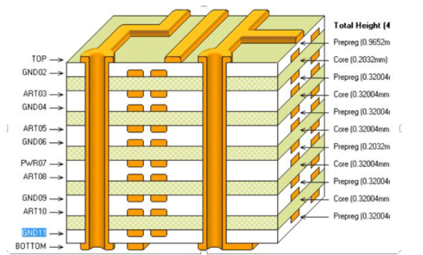
A multilayer printed circuit board is a circuit board composed of two or more conductive layers (copper layers) superimposed on each other. The copper layer is bonded together by a resin layer (semi-cured sheet). Multilayer PCB board is the most complex type of printed circuit board. Their price is relatively high due to the complexity of the manufacturing process, low volume of production, and the difficulty of rework.
Do you know how are multilayer pcbs manufactured? Due to the increase of the density of the integrated circuit package, the high concentration of the interconnect leads to the use of multi-substrate becomes necessary. In the case of a large number of interconnect and crossover requirements, the PCB board must be expanded to more than two layers in order to achieve a satisfactory performance, so the multi-layer PCB appears.
This is how are multilayer pcbs manufactured. The primary purpose of multilayer circuit boards is therefore to provide more freedom to choose the appropriate routing paths for complex and/or noise-sensitive electronic circuits. The multilayer PCB board has at least three conductive layers, two of which are on the outer surface, while the remaining layer is synthesized inside the insulation board. The electrical connection between them is usually achieved through plated through holes in the cross-section of the circuit board.
Advantages Of Multilayer PCBs
There are many multilayer PCB advantages. Multilayer PCB commonly used in high-speed PCB design, the fabrication process of multilayer PCB production is laminating the etched single or double PCB, then glue them into a multilayer PCB, compared with single or double layers PCB, there are a lot of advantages, especially in a small volume of electronic products, here are the multilayer PCB advantages.
- Small Size, making the PCB size smaller due to multi-layer design.
- Reduce Weight, reduces the need for interconnection wiring harnesses and uses smaller PCB to reduce the weight.
- High Assembly Density, high density components on the multilayer PCBs that enable greater capacity, and speed.
- High Quality, the stable quality of multilayer PCBs is better than single-layer and double-layer PCBs.
- Good Flexibility, adopted a flexible construction technique to increase flexibility.
- Improve the Speed of Signal Transmission, the wiring between the electronic components of the multilayer circuit board is shortened, improves the speed of signal transmission.
- Better Shielding Effect, High-frequency and multilayer circuit, after joining the ground layer, the signal line will form a constant low impedance to the ground, and the circuit impedance will be greatly reduced.
Disadvantages Of Multilayer PCBs
- Higher Cost, multilayer PCB is much more expensive than single-layer PCB and double-layer PCB duo to the design and production is more complex.
- Complex Production, multilayer PCB manufacturing process and equipment required more accuracy, so the production is more complex.
- Longer production time, as the complexity and manufacturing requirement increases, so the fabrication time required more.
Applications Of Multilayer PCBs
- Consumer Electronics
- Computer Electronics
- Communication Electronics
- Industrial Control
- Medical Devices
- Automotive Electronics
- Aerospace Electronics
- Military and National Defense
- Internet of Things
Multilayer PCB Design Tips
- PCB planning:Planning PCB shape and size, number of board layers, component packaging, component installation in advance.
- Setting working parameters: Setting PCB environmental parameters correctly and reasonably to improve the efficiency of PCB design.
- Component placement: Component placement is an important step in multilayer PCB design, components can be placed as neatly and beautiful as possible, at the same time, placement reasonable or not, will directly affect the performance of the PCB, so in the layout of the schematic diagram should be carefully analyzed to avoid mistakes.
- Segmentation of power layer and GND layer: Multilayer circuit boards have different power supply layers and connections. The power supply layers must be separated and connected to the specified power supply network due to the voltages are connected to the same power supply layer.
- Wiring: Multilayer PCB design is carried out according to circuit function. During wiring, special attention should be paid to wire width, spacing, safe spacing between wire and solder pad and the size of vias, etc. Good wiring can not only ensure the performance of the circuit board, but also meet the technical requirements of manufacturers.
- DRC, DFM inspection, and document output: After the PCB design is completed, DRC and DFM should be carried out to check whether the design is feasible. Then output Gerber, BOM, Pick &Place file, and other relevant documents to PCB manufacturer for inquiry.
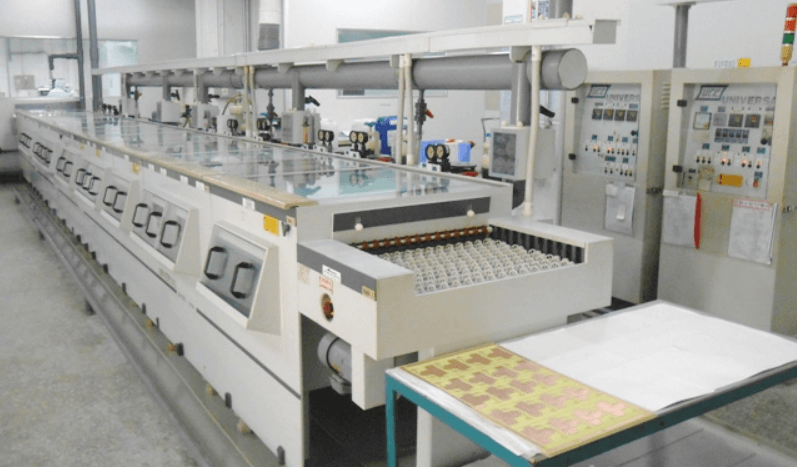
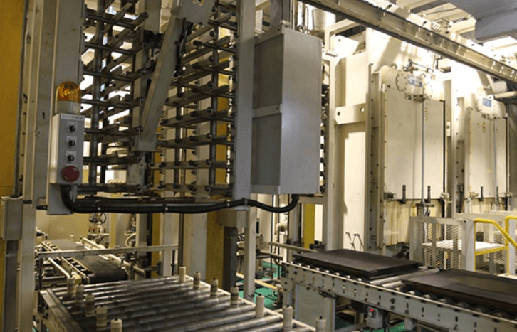
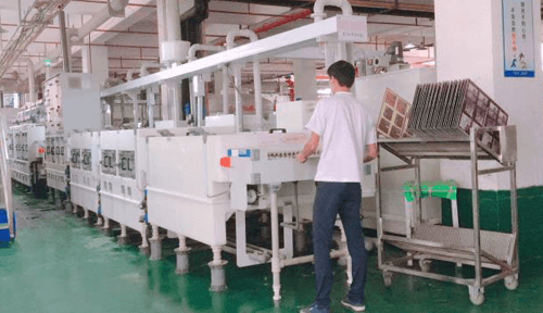
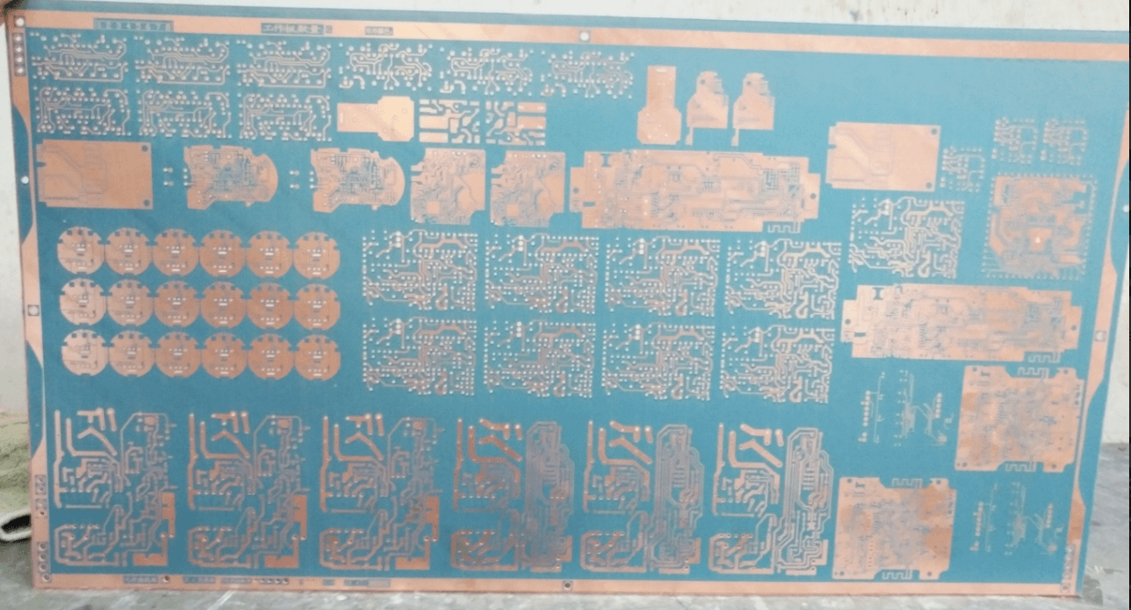
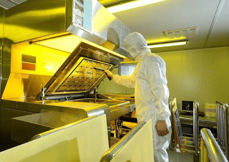
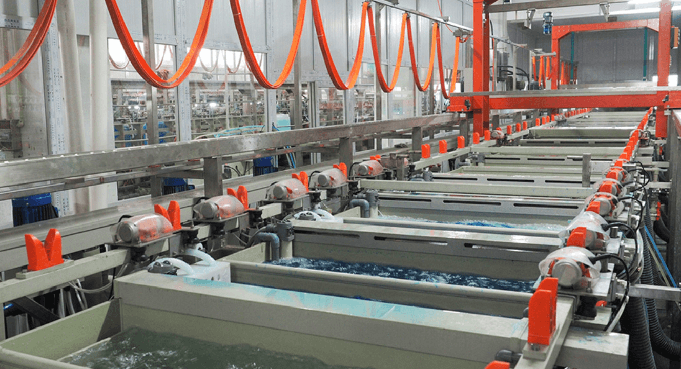
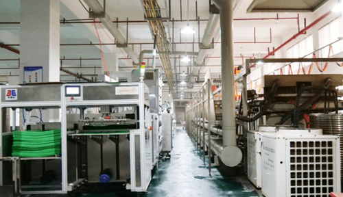
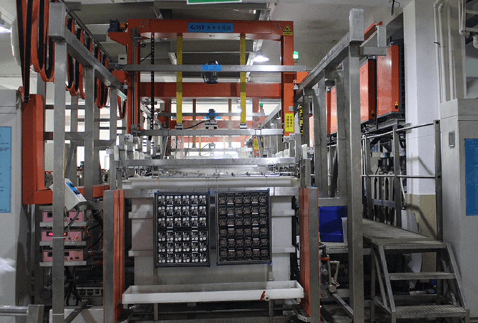
Multilayer PCB Manufacturing Process
Multilayer PCB is composed of two or more layers of circuit boards. The multilayer PCB manufacturing process is more complicated than other circuit boards. Let’s take a step by step look at the multilayer PCB manufacturing process.
1.Board Cut
The first step of multilayer PCB manufacturing process is according to the order requirements, cut substrate into the size specified by MI.
2.Inner Layer Dry Film
Transferring the inner layer circuit pattern to the PCB board.
3.Pretreat
The contaminants on the copper surface are removed and the roughness of the copper surface is increased to facilitate the subsequent pressing film multilayer PCB manufacturing process.
4.Inner Layer Lamination
The copper surface of the treated substrate is affixed with an anticorrosion dry film by hot pressing.
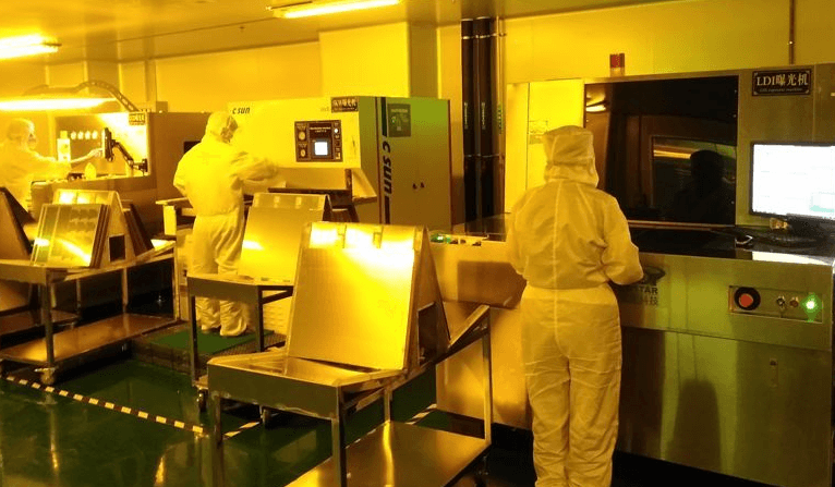
5.Exposure
In the exposure machine, ultraviolet light is used to transfer the negative image to the photosensitive dry film.
6.Developing
The dry film without chemical reaction was washed away by lye, and the exposed part was retained.
7.Etching
The copper exposed after developing is etched away with acid copper chloride to form the inner layer circuit pattern and obtain the desired circuit.
8.Strip
The exposed dry film protecting the copper surface is peeled off with sodium hydroxide to reveal the circuit pattern multilayer PCB manufacturing process.
9.Brown Oxidized
It makes the inner copper surface form a microscopic rough and organic metal layer, and enhances the bonding strength between the inner copper layer and prepreg.
10.Lay-up
Bonding all copper layers with the help of the adhesive properties of PP.
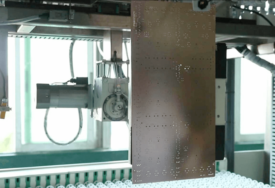
11.Drilling
Through holes are produced between the circuit board layers to achieve the purpose of connecting the layers.
12.Plated Through Hole
Through a series of chemical treatments, a uniform layer of metal copper is formed on the through-hole wall and the copper surface of the plate, to achieve electrical communication between the layers multilayer PCB manufacturing process.
13.Panel Plating
Thicken the copper in the hole wall and the plate surface to a certain thickness to prevent the copper in the hole from being oxidized or eroded and leaking the substrate before graphic electroplating.
14.Outer Layer Dry Film
Same as the step of inner layer dry film.
15.Outer Layer Pattern Plating
Graphical electroplating copper after the transfer of graphics, through the way of electroplating on the hole and the line electroplating treatment, to meet the final request of copper thickness.
16.Solder Mask
As a protective layer, the solder mask is coated on the wire and the substrate to expose the pads and holes, to prevent short circuits during soldering.
17.Silkscreen
The required text, logo, or part symbol is printed on the board, and then exposed to ultraviolet light on the board.
18.Surface Finish
Bare copper exposed to the air for a long time is easy to oxidize, to ensure good solderability or electrical properties, surface treatment of copper is needed, common surface finish: HASL, ENIG, OSP, immersion tin, Immersion silver, hard gold, etc.v
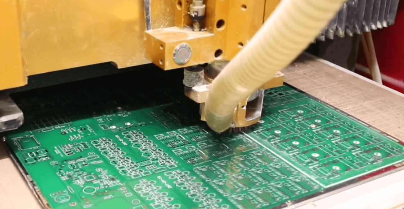
19.Outline
Cut the PCB into the required dimensions with a CNC machine.
20.Electrical Testing
Simulate the state of the board, proceed with an electrical performance check, whether there is an open, short circuit.
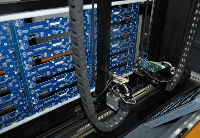
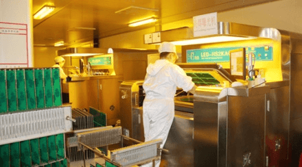
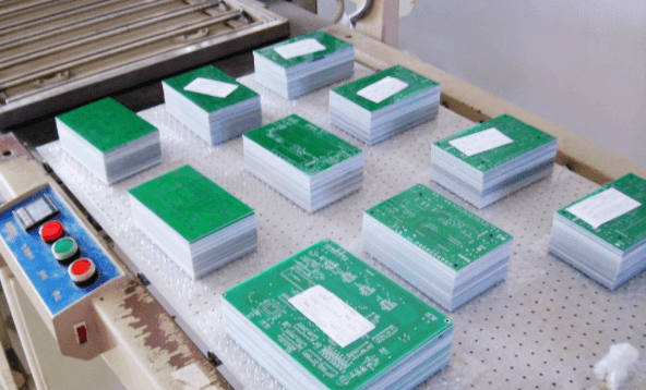
21.FQA & Packing
The last step of multilayer PCB manufacturing process is to check the appearance, size, hole, thickness, and other marks of the board to meet customer requirements. The qualified products will be packaged into a vacuum package and shipped to customers.
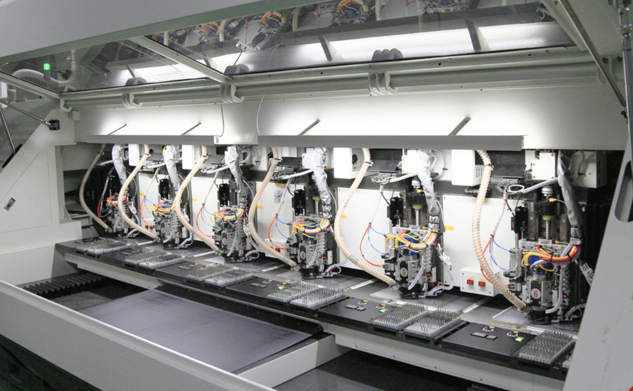
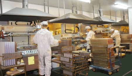
The above is the detailed steps of the Multilayer PCB Manufacturing Process. The process of multilayer printed circuit board requires specialized equipment and strict requirements for operators. This explains why some pcb board manufacturers are slow to enter the multilayer circuit board market.
Summary
Well, Now you have a basic understanding of the multilayer pcb and multilayer pcb manufacturing process. With the development of society, our demand for multilayer pcb design has been on the rise. The multilayer pcb board has created a new world. You can only use it better if you understand it more seriously.