Introduction
In this article, I will introduce pcb basic knowledge for you. Basically, pcb printed circuit boards appear in every kind of electronic equipment. If there are electronic parts in a certain kind of equipment, they are all embedded on PCBs of different sizes. In addition to the various small fixed parts, the main function of the PCB is to provide electrical connections between various parts. If you want to learn more about pcb, then you should first learn about pcb basic knowledge.
pcb overview
pcb structure
The first pcb basic knowledge. And this is pcb basic knowledge you must know. Single-sided board: It is a circuit board with copper-clad but no copper-clad on the other side. Users can only route and place components on the copper-clad side.
Double panel: The double panel includes the top and bottom layers. The top layer is generally the component surface, and the bottom layer is generally the solder layer. Both sides of the double-sided board can be copper-clad or wired.
Multilayer board: A circuit board containing multiple working layers or power layers, generally refers to a circuit board with more than three layers. In addition to the top layer mentioned above, the bottom layer unexpectedly also includes the middle layer, internal power supply or ground layer, etc.
Component packaging
The second pcb basic knowledge. How to ensure that the pin of the component is consistent with the solder plate on the pcb printed circuit board? This depends on component packaging.
Component packaging refers to the appearance and location of the pads when the component is soldered to the circuit board. Component packaging is only a concept of space. Therefore, different components can be packaged with one component together; in addition, the same component can also have different packages, such as resistors.
Copper film wire
The third pcb basic knowledge. Copper film wires are also called copper film wires, referred to as wires. It is used to connect each pad and is the most important part of the PCB. PCB design revolves around how to lay out the wires.
Related to the wire is another kind of wire, often called a flying wire. That is, the pre-pull wire. The flying line is generated by the system according to the rules after the netlist is introduced, and is used to guide the wiring of a kind of connection.
Solder Flux Film and Solder Mask
The fouth pcb basic knowledge. Various types of films are not only indispensable in the PCB manufacturing process, but also necessary conditions for component soldering.
According to the position of the film and its function, the film can be divided into two types: component surface soldering film and component surface solder mask.
The soldering film is a film applied on the pad to improve the solderability, that is, a light-colored circle slightly larger than the pad on the green board. The solder mask is just the opposite. In order to make the board suitable for wave soldering and other soldering forms, the copper foil on the board other than the pad must not be tinned. Therefore, a layer of paint must be applied to all parts other than the pad. To prevent tin on these parts.
Pads and vias
The fifth pcb basic knowledge.
Pad: The function is to place solder and connect wires and component pins. The pad is the most frequently contacted and most important concept in PCB design. The pads have round, square, elliptical, rectangular and other shapes.
Via: It is the line connecting each layer. Drill a common hole at the intersection of the wires that need to be connected in each layer, which is a via. There are three types of vias, namely through-holes from the top layer to the ground layer, blind vias from the top layer to the inner layer or from the inner layer to the bottom layer, and hidden vias from the inner layer.
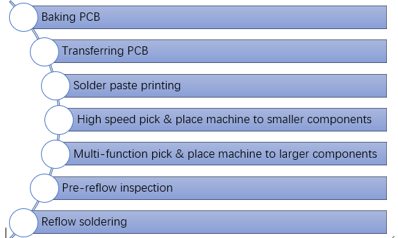
What is SMT assembly process?
SMT assembly process is also pcb basic knowledge you should know. The process of SMT is as follows:
Baking PCB
Transferring PCB
Solder paste printing
Solder paste inspection (SPI)
High speed pick & place machine to smaller components
Multi-function pick & place machine to larger components
Pre-reflow inspection
Reflow soldering
AOI
Visual inspection
What costs are involved in PCB assembly?
This paragraph is about pcb basic knowledge about PCB assembly cost.
Except for the electronic components cost and assembly cost, there has engineering costs and stencil costs. Before the PCB assembly process, there is going to do a lot of preparation work, electronic components checking compared with BOM, pick & place machine programming, and AOI programming
Whether it is 10-20 pieces of the sample or mass production, these processes have to be done, we call it engineering costs. And the first step of assembly is applying solder paste on PCB, so the stencil is needed. If there is a certain amount of order and THT plug-in is to be made, it is necessary to go through wave soldering.
After wave soldering, the fixture should be provided, which can better guarantee the quality of soldering and also improve production efficiency. For the stencil and fixture costs, if not modified PCB data, generally only charged one time on the first order, UETPCBA will keep them 3 months for customers.
How long is the delivery time of PCBA orders?
This paragraph is about pcb basic knowledge of delivery time of PCBA orders.
The delivery time of PCBA orders is calculated when all electronic materials are ready. The OEM PCBA orders depend on the delivery time of the electronic materials (generally the overseas purchased materials take a relatively long time). If all the electronic components have been prepared, the delivery of small PCB assembly orders (1-200pcs) can take 3-4 days in UETPCBA, while the delivery of large PCB Assembly orders (200-1000pcs) take 5-7 days.
Why need AOI, X-Ray and FCT tests?
This paragraph is about pcb basic knowledge of testing.
AOI test in PCB assembly is mainly used to inspect whether electronic components damaged, short, misalignment, solder bridge, solder empty and non-solder, etc. generally after SMT reflow soldering, AOI test should be done.
X-Ray is mainly for the PCB with BGA after the chip is soldered, generally just sampling inspection.
FCT functional test is mainly to inspect the electronic input and output parameters of the assembled PCBA to make sure the boards work as expected, which requires the customer to provide the program or the electronic engineer of UETPCBA to cooperate with the customer to develop the testing program.
Why weprefer to do OEM PCB Assembly orders?
This paragraph is about pcb basic knowledge of OEM PCB Assembly.
The main reason is to help customers save costs and avoid the trouble of purchasing materials and avoid quality problems in case of disagreement. UETPCBA has established a relatively perfect and efficient electronic components supply management system. Our procurement channels are regular, which can guarantee quality, offer favorable prices, and save costs for customers.
We do not need to spend time and effort on purchasing electronic components. At the same time, if there is any quality problem, whether it is material problem or a PCB assembly problem after the delivery of the PCBA order, we will be responsible for it.
However, if the PCBA processed with supplied materials has quality problems, it may be due to the poor soldering of PCBA, or it may be due to the poor quality of supplied materials, and the responsibility lies with the customer. To avoid and reduce the differences in solving quality problems, it is more beneficial for the customer to choose an OEM PCBA factory instead.
Summary
Well, the above is about pcb basic knowledge, which involves PCB assembly, PCBA orders and testing. The mastery of pcb basic knowledge is the first step for you to understand pcb. There are many contents about pcb basic knowledge and hen not presented. About pcb basic knowledge, this article will stop here. If you want to know more pcb basic knowledge, please feel free to consult us.