Overview
In order to make the description simple, there will be very professional pcb terms in many texts. Maybe you don’t know much about pcb terms. A basic understanding of pcb terms related professional knowledge can make it easier to cooperate with printed circuit board manufacturers. In this post, I’ll show you some common pcb terms.
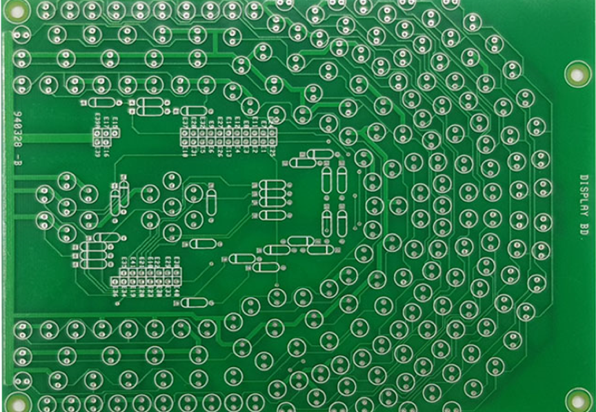
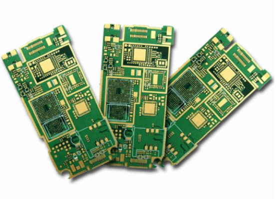
PCB
PCB is the most basic PCB term. PCB also known as Printed Circuit Board, is an important electronic component, which is the carrier of electrical connection of electronic components. Printed Circuit Board is designed to be small, lightweight, reliable and easy to maintain.
FR-4
FR-4 is a fire-resistant material grade code, which means that the resin material must be able to extinguish itself after the combustion state of a material specification, the general circuit board used fr-4 grade materials are very many kinds, but most fr-4 are composites made from what is known as tera-function epoxy with Filler and glass fiber.
Copper
The copper foil layer is very thin and is pressed onto the substrate by heat and binder during production. When we talk about double PCB, we mean we have two pcb copper layers on the surface. Copper layer thickness is more varied, and is in weight units, generally used to cover the weight of one square foot of copper evenly (oz) to express.
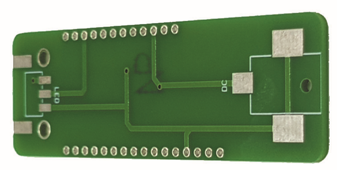
Solder Mask
This is a layer of material, which is used for the entire printed circuit board. Solder Mask helps to physically and electrically insulate the traces to prevent short circuits. Above the copper layer is the solder mask layer. This layer makes the PCB appear green or other colors. The solder mask covers the wiring on top of the copper layer to prevent the wiring on the PCB from contacting other metal, solder, or other conductive objects and causing a short circuit. The presence of a solder mask allows you to weld in the right place and prevents solder bridges.
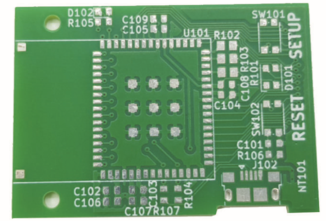
Silkscreen
The pad numbers and symbols are printed on the solder mask layer, so that easy to distinguish which components are soldered on the right pads, and facilitate assembly. We often use the symbol of the silkscreen layer to mark some pins or LED functions. The silkscreen layer is the most common color is white.
Pad
As a pcb term, pad is a kind of metal exposed on the surface of a PCB used to solder components. Multiple Pads are used together to generate component packages or land patterns on the PCB.
Through Hole
Through Hole refers to a hole passing through at least two PCB layers. The holes run through the entire printed circuit board and can be used for internal interconnections or as mounting and locating holes for components. the lower cost and the easier drilling, so most printed circuit boards are used, rather than the other two kinds of through hole. Generally referred to as through holes, without special instructions, are considered as through holes.
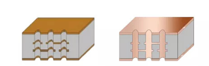
Buried Hole
Refers to the local through hole of the multilayer board, when it is buried in the inner layer of the multilayer board becomes the “inner through hole”, and is not “connected” with the outer plate, called the buried guide hole or referred to as the buried hole.
Blind Hole
In a complex multilayer PCB, some of the through-holes are deliberately not fully drilled because only a few layers of interconnection are needed. If one of the holes is connected to the ring of the outer plate, such a special hole like a cup-shaped Blind alley is called a “Blind Hole”.
PCB Layout
PCB layout is also a PCB term that many people don’t understand. Based on comprehensive consideration of signal quality, DFM, EMC, thermal design, DFT, structure, safety requirements, and the components are placed on the board reasonably. It is an important step to achieve wiring, the good layout can effectively achieve PCB all signal distribution.
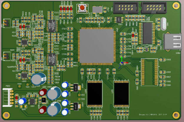
Routing
The operation of connecting all electrical connections with actual wiring according to the network table and design requirements after the layout is complete. PCB design usually uses manual intervention for automatic wiring.
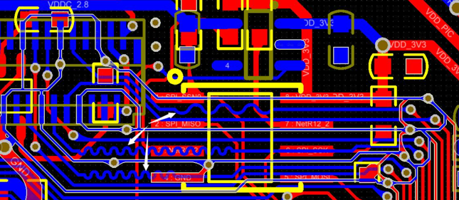
Basic Grid
Refers to the circuit board in the design, the conductor layout location of the vertical and horizontal grid. The early lattice spacing was 100 mil, but now the basic lattice spacing has been reduced to 50 mil due to the prevalence of thin and dense lines.
BGA
Ball Grid Array (BGA) technology is a surface bonding packaging technology used in integrated circuits, which is commonly used to permanently fix devices such as microprocessors. The BGA package can accommodate more pins than other packages such as the Dual-in-line package or Quad Flat package. It also has a shorter average wire length than the surrounding limited package type for better high-speed performance.
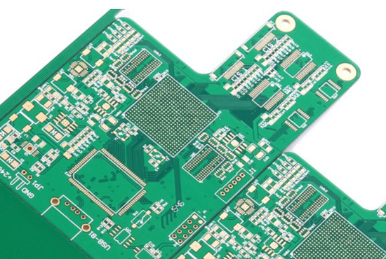
HDI
HDI stands for High Density Interconnector. It is a printed board with high circuit density that uses the micro-blind buried hole technology. HDI is designed for compact and small volume products.
Conclusion
A basic understanding of some commonly used pcb terms can make printed circuit board manufacturing companies work faster and easier. This article on pcb terms will help you understand some commonly used terms in the industry. Although not comprehensive, it is a good resource for your reference.