The electroplated copper layer is one of the essential electroplating technologies in PCB manufacturing because of its good electrical conductivity, thermal conductivity and mechanical ductility.
Reasons for plated through hole pcb
Through-hole technology has various advantages, which helps its popularity among electronics manufacturers.
Simple prototyping: using plated through hole pcb can achieve faster prototyping than SMT. The pin through-hole component can be soldered to the board by hand soldering or wave soldering.
Excellent physical connection: The pth pcb board helps to establish a strong mechanical bond between the component and the circuit board. Through-hole technology is used to install components that must withstand mechanical stress, high power and high voltage.
High power tolerance: plated through hole pcb can easily meet high power requirements. Through-hole components work with the circuit board, and they can easily withstand mechanical and environmental pressures.
Component durability: Through-hole mounting helps to establish a strong physical bond between components. These components are firmly soldered on both sides of the circuit board, and the pth hole in pcb helps to improve its durability.
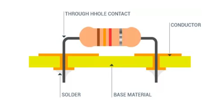
Plated Through Hole (PTH) is used to make the non-conductive part of the resin and glass fiber on the wall of the
hole to metalize (metalization) for the later process of copper plating to complete the conductive and welding metal hole wall.
Plated through hole, the PCB via hole must be plugged. A Via hole acts as a conduit for interconnecting lines. In 1986, an American chemical company Hunt, announced that PTH did not need the traditional metallization process of precious metals and electroless copper, and instead used toner as a medium for electrification.
The through hole should meet the following requirements:
- Make sure there is copper plated into the wall of through hole
- No solder mask goes into the hole to avoid tin beads in the hole
- The through hole must have solder pth pcb board, light proof, no tin ring, tin bead.
Three main functions of the through hole
- Prevent in PCB wave soldering tin from the through hole through the surface of the components caused by short circuit.
- Prevent the solder paste flowing into the hole, leading to poor soldering and affecting the mounting;
- Prevent flux residue in the through hole;
pcb pth process
- Deburr: After drilling the hole, if the drilling conditions are not appropriate, 1) the copper wire at the edge of the hole is not cut; 2) Residual of uncut glass fiber (BURR)
- Desmear: Four methods of removing the desmear: 1) Sulferic Acid, 2) Plasma, 3) Cromic Acid, 4)Permanganate
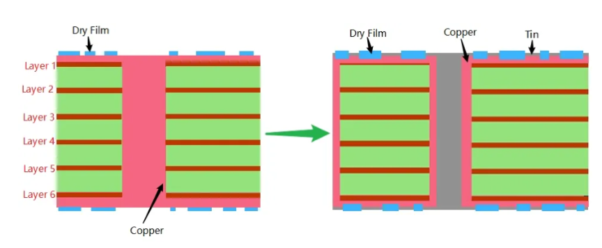
- The plated through hole
- First copper
- The last step of plated through hole: secondary copper
Conclusion
All the points mentioned above help to understand the popularity of plated through hole. You must obtain PCB components from trusted manufacturers who understand your requirements and provide you with appropriate solutions. Through hole vias pcb has extensive experience in designing and building PCB components for various industrial electronic applications.