HDI pcb definition
The high density interconnect pcbs known as the hdi pcbs or hdi printed circuit boards, is one of the indispensable electronic components in electronic devices.
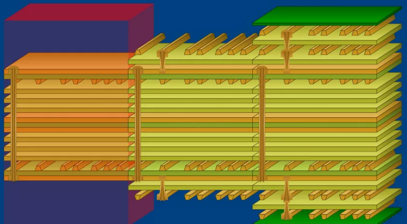
The definition of HDI circuit board refers to the microvia (Microvia) with the hole diameter below 6mil (0.15mm), the hole ring diameter (HolePad) below 0.25mm, the contact density is above 130 points/square inch, and the wiring density is less than Printed circuit boards above 117 inches/square inch, and whose line width/spacing is less than 3mil/3mil.
Development of HDI pcb
High density interconnect pcbs processing technology has been used in pcb design since it was first applied to semiconductor packaging modules in the late 1980s. Today, laser drilling with controlled depth in laminates, combined with a range of copper plating processes, is the primary method of manufacturing HDI.
PCB boards started around the 1960s, are usually produced from resin substrate electroplated through-hole PCB. Because of its production copy fast, small size, low unit price characteristics replaced the early wire assembly products.
With the miniaturization of electronic equipment, components are also compact and miniaturization, and then developed BGA (Ball Grid Array), CSP, DCA, and other parts, which makes the circuit board to an unprecedented high-density condition. To meet the requirements of high density, the microporous structure is used to improve assembly and space utilization. For this type of circuit board, it is called adding layer multilayer board.
When the communication frequency is increased again, the added layer multi-layer board can not meet the needs. To improve the connection density of components, geometrically compress the circuit and connection point space, or stack multiple components in the same position to improve the construction density. This technology is known as high density interconnect pcbs, or hdi technology.
HDI PCBs application scenarios
Currently, the main application scenarios of hdi pcb technology include carrier and intermediary boards, modules, portable products, and high-performance products.
1) Carrier and intermediary board: HDI technology is used in overlaying or wiring applications, where the microporous design allows very high density overlaying areas to construct the contacts and winding of an array configuration.
2) Module: HDI technology can be used to build modules that allow IC to be wired, overlaid or tabbed on a small carrier, or it can be used to create detailed CSP.
3) Portable products: Portable products and miniaturized consumer products using HDI technology are smaller in shape and have more detailed characteristics.
4) High-performance products: The hdi circuit boards is used in conjunction with the microporous structure for the manufacture of high level, high I/O, small spacing components, especially high-density components.
Advantages of HDI PCBs
The introduction of HDI technology brings many benefits in wiring configuration, component arrangement, material selection, product design, and manufacturing processes, all of which are indicators of product intent. The specific benefits of high density interconnect pcbs are:
Performance improvement
Typical performance improvement includes:
- Presents relatively low parasitic electrical noise from the through-hole
- Minimize the connection hole and line branching structure
- HDI pcbs have a stable voltage path
-
High density pcb can remove unnecessary de-coupling capacitors
-
HDI circuit boards have low conversational style and general noise
- RFI/EMI interference is much lower
- The near grounding plane, the near capacitance distribution
- The surface grounding plane is equipped with holes in the cushion structure, which can block the radiation effect
Import advanced components
When using IC structures with 0.8mm spacers, HDI pcbs has a significant advantage over laminates. For example, with field-programmable gate array (FPGA) high-pin products, the through-hole technology may require more than 20 layers, whereas with HDI it requires only about 60% of that. In addition, HDI technology blind hole saves the inner layer and a hole liner space, also can do hole in the cushion design.
Faster time to market:
HDI technology uses the blind hole and the hole in the pad structure, convenient electronic component configuration, and shortens the time to market. At the same time, this design occupies less space, the product design space efficiency is increased, the application performance of BGA components is improved, the winding flexibility is increased, and the circuit design is more simple.
In addition, the use of blind and buried design to improve electrical performance can greatly shorten the time for system design adjustment, reduce signal integration and noise reduction, and reduce the chance of redesign.
Improve reliability:
Compared with the traditional through-hole, the aspect ratio of the blind hole is mostly less than 1:1, while the traditional through-hole is in the range of 4:1 to 20:1. This enables the blind/microporous structure to have high serial number transmission reliability.
In addition, the thin structure of the high density pcb, low z-axis expansion coefficient material, makes the hdi pcbs has low potential inductance and good heat conduction ability.
Lower costs:
Using hdi technology can reduce the number of board design layers, improve component density, and improve system speed and impedance performance. Therefore, combined with the hdi multi-layer structure, the cost is lower than traditional through hole pcb.
HDI pcb design guidelines
HDI pcbs are designed by hdi pcb manufacturer to maximize surface component density, provide breakthrough solutions for ICs with large numbers of tightly-spaced pins, or transmit high-frequency signals.
HDI pcb design is very complex, and PCB designers should optimize the manufacturing of hdi pcb designs based on the difficulty of pcb production. Here are some hdi pcb design guidelines.
- It’s better to design through-hole types to minimize production complexity and cost savings
- Component selection and optimization are important to HDI PCBs
- Space components minimize stress and EMI
- Routing should minimize signal integrity issues
- Design appropriate PCB stack-up to minimize material costs
HDI pcb manufacturer
UETPCBA
As an hdi pcb manufacturer, UETPCBA has advanced pcba manufacturing equipment and leading technology. Moreover, UETPCBA provides a wide range of hdi pcb services to customers from different countries.
Shennan Circuit Co., Ltd.
The company was established in 1984 and mainly produces hdi printed circuit boards. The number of employees is huge.
Guangdong Shantou Ultrasonic Printing Plate Company
As an hdi pcb manufacturer, the company has many years of experience and a professional team, you can send your needs to the company.